Mapping 2D Ferroelectric Materials Unveils Connections
Mapping 2D Ferroelectric Materials Unveils Connections

Identifying structural features of 2D ferroelectric materials could influence the design of next generation nanoelectronics.
Scientists at Rice University have mapped the structural features of 2D ferroelectric materials, which are a class of materials that exhibit spontaneous electric polarization that can be reversed in direction by the application of an external electric field. This knowledge may help researchers with the design of more advanced nanoelectronics.
Ferroelectrics are often compared as the electrical analog to ferromagnets and are both piezoelectric and pyroelectric. They’re widely used in a variety of electronics applications, including semiconductors, SSDs, sensors, and capacitors. Manufacturers of these devices use ferroelectric materials not only for the reversable polarization but because of their lattice structure, atomic thinness, and enhanced integration capabilities.
Mapping the properties in a new 2D ferroelectric material made of tin and selenium atoms provides new insight into how they are connected. This may lead to new ways to use existing materials or the design of new ones. The multi-year-long effort is documented in a new study published in Nature Communications, “Domain-dependent strain and stacking in two-dimensional van der Waals ferroelectrics.”
 Yimo Han (left) and Chuqiao Shi. Photo: Gustavo Raskosky/Rice University
Chuqiao Shi, a Rice graduate student working in collaboration with Yimo Han of the Han Lab, is the lead author of the paper and part of a broader team studying 2D ferroelectric materials.
“This is a new material. We call it van der Waals ferroelectric material,” said Shi. These 2D ferroelectrics can change shape in response to electrical stimuli, known as flexoelectricity. In the mapped tin-selenium crystal, molecules self-organized into patches or domains. The flexoelectric effect causes them to move, creating structural shifts that impact their properties and behavior.
Become a Member: How to Join ASME
The forces that bind the atoms are weaker, giving the material more pliant and flexible qualities. This provides an advantage over conventional ferroelectric materials, where atoms are bound by a rigid lattice structure. Trying to meet the demand of microelectronics manufacturers for ever thinner and smaller materials is challenging with conventional ferroelectric materials because they lose their internal polarization once they exceed a few nanometers in thickness.
“That's a new trend in this field because people always want it smaller and simpler,” said Shi, explaining how van der Waals ferroelectric materials can be applied. “Even though it gets thinner and thinner in modeling, it still has a strong polarization,” he added.
The team’s next steps include looking into where else the 2D ferroelectric materials may be applied, Shi said. Another challenge is creating a path to fabricate them on a large scale.
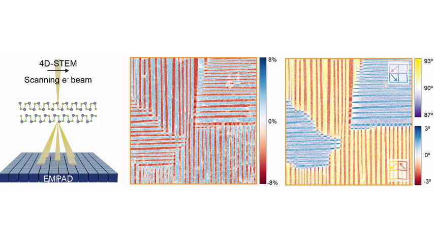 Researchers used 4D scanning transmission electron microscopy to analyze the material's structure (left). Analysis yielded a ferroelastic strain map of a material flake (center, right). Insets on the right represent polarization directions in different stripe domains. Image: Han Lab/Rice University
The flexibility found within the atomic lattice in the 2D van der Waals ferroelectrics creates challenges in discovering the relationships between polarization and material structure.
Shi said the challenges are exciting because the team is using a new technique that involves 4D scanning transmission electron microscopy. In traditional scanning, there is one pixel—one of three RBG numbers, he explained.
“But in the 4D, in one pixel, it contains the full images,” said Shi. Even though 4D scanning results in a large and sometimes “very messy” amount of data that may be up to five times larger than what comes from a traditional scan, it enables scientists to find the structure. “That we can find it is the most important thing,” said Shi.
In the paper’s conclusion, the authors noted this “approach surpasses the constraints of traditional imaging techniques,” allowing for “simultaneous mapping of in-plane and out-of-plane structure across the entire flakes.” Their findings may have profound implications in influencing switching energy and their viability in memory and actuator device applications.
The greater collaboration with others outside of Rice and the Han Lab is another aspect of the work that excites Shi. The Rice team worked with Ye Cao from the Department of Materials Science and Engineering at the University of Texas, Arlington, who provided phase-field simulation to explore and understand how the domain structures create energy. Xiaofeng Qian from the Department of Materials Science & Engineering at Texas A&M University provided simulations that helped the Rice team understand the atom positions.
“We have had several very productive discussions in this process,” said Shi. “It's a good chance for me to learn from them.”
Nancy Kristof is a science writer in Denver.
Related Content