New 3D Printing Method Cuts Material Development Time in Half
New 3D Printing Method Cuts Material Development Time in Half
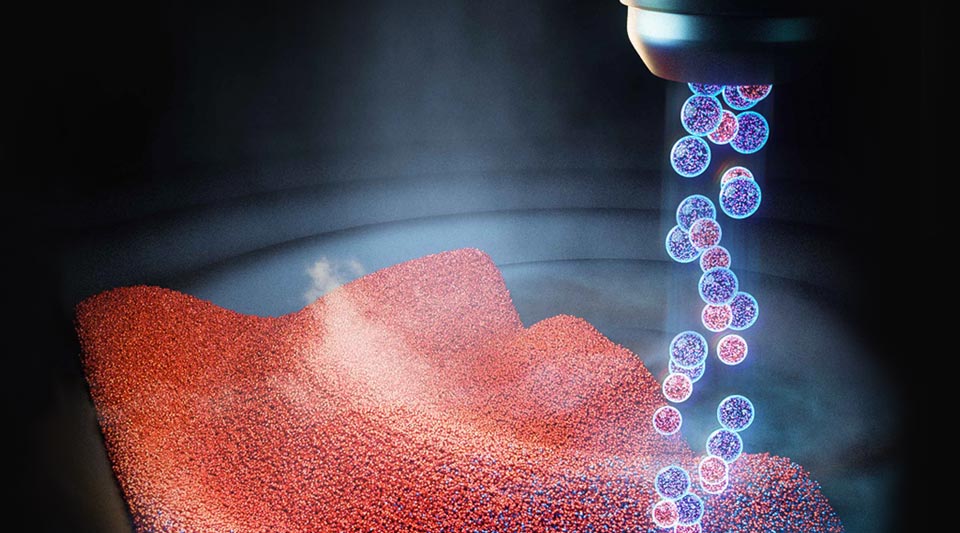
High-throughput combinatorial printing illustration. The new 3D printing method drastically accelerates the discovery and production of new materials.
The speed of material development must keep pace with technology advancements to maintain R&D and the rate of discovery and invention. High-tech, next-generation technologies such as clean energy, biomedicine, nanoelectronics, and environmental sustainability depend on new materials with highly-specific mechanical and chemical properties. However, material discovery and commercialization is still mostly a trial-and-error process that is slow, labor-intensive, and expensive, especially for nanomaterials.
Using these traditional approaches, it typically takes 10-20 years to discover, test, and commercialize a new material. To accelerate this process, a University of Notre Dame research team led by Yanliang Zhang, associate professor of aerospace and mechanical engineering, decided to explore ways of using additive manufacturing (AM) to speed up the development of new nanomaterials.
“I thought if we could shorten that time to less than a year—or even a few months—it would be a game changer for the discovery and manufacturing of new materials,” says Zhang.
High-throughput combinatorial printing
The first step was developing a more effective 3D printing method.
“Several printing approaches, including inkjet printing, electrochemical printing, and electrohydrodynamic redox printing, have been proposed for the fabrication of material libraries,” says Zhang. “However, these methods still suffer from limited materials options and challenges in regard to the universal combination of different materials and the production of gradient material libraries, due to the lack of fast mixing mechanisms and the inability to rapidly vary mixing ratios.”
To remedy this deficiency, Zhang and his team developed a 3D printing process they call high-throughput combinatorial printing (HTCP). Because the process works best with low fluid viscosities, the team focused on using aerosols for in situ mixing and printing. Aspects they explored included ink formulation, aerosol mixing and interaction, and printing parameter optimization, using methods such as fast camera imaging and computational fluid dynamics simulations.
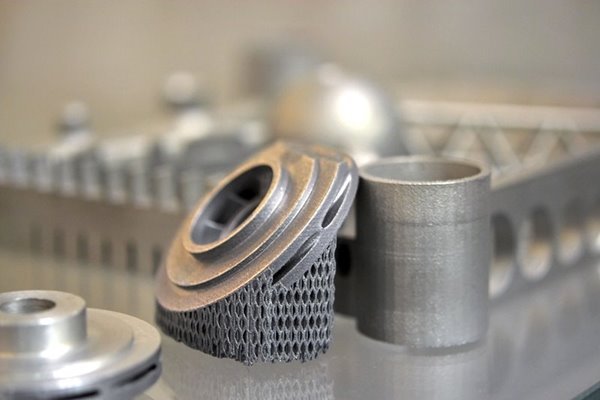
Design for Additive Manufacturing
The HTCP method can combine two or more aerosolized nanomaterial inks in a single printing nozzle. During the printing process, the ink-mixing ratio can be adjusted on the fly to create materials with specific properties and gradient compositions at microscale spatial resolution.
“The HTCP process begins with atomization of two or more inks into aerosols containing microscale ink droplets, where the combined ink streams are then mixed in a single nozzle and aerodynamically focused by a co-flowing sheath gas before deposition,” says Zhang. The aerosol jet printhead then prints fine features with spatial resolution as low as 20 µm in the x-y plane and deposition thickness as low as 100 nm.
As an example, the team printed a metal/semiconductor nanocomposite using an Ag nanoparticle ink and a Bi2Te3 nanoplate ink. Once the narrow stream of mixed aerosols was formed, “we gradually increased the metal-to-semiconductor ink-mixing ratio and observed a clear morphological transition from a Bi2Te3 nanoplate-rich phase to a well-blended composite phase and then to an Ag nanosphere-rich phase,” Zhang adds.
Versatile and applicable
The aerosol-based HTCP method can be used with a broad range of materials, including metals, semiconductors, and dielectrics, polymers, and biomaterials. Some of these combinational materials can serve as “libraries,” each containing thousands of unique compositions. Perhaps the most innovative aspect of HTCP is that it can print functionally graded materials that transition from stiff to soft—properties that are especially useful in biomedical applications such as catheters designed for certain parts of the body, lattices that connect soft body tissues to stiff wearable and implantable devices, and surgical tools for minimally invasive procedures.
Zhang’s team has already used HTCP to generate a semiconductor material with superior thermoelectric properties—a promising discovery for energy harvesting and cooling applications.
“The next phase of our work will be leveraging the fabrication freedom and data-rich nature of HTCP, along with machine learning and artificial intelligence-guided design strategies, to accelerate the discovery and development of a broad range of materials with unprecedented properties for emerging applications,” says Zhang. “Ultimately, I hope to develop an autonomous and self-driving process for materials discovery and device manufacturing, so students in the lab can be free to focus on higher-level thinking.”
Mark Crawford is an independent writer in Corrales, N.M.

Stay up to date on the advances in additive manufacturing. This collection highlights new applications of 3D printing, metal printing methods, materials development, medical devices, and bioprinting.