Tiny Ski Jumps Open a Path for Photonic Chips to Scale
Tiny Ski Jumps Open a Path for Photonic Chips to Scale
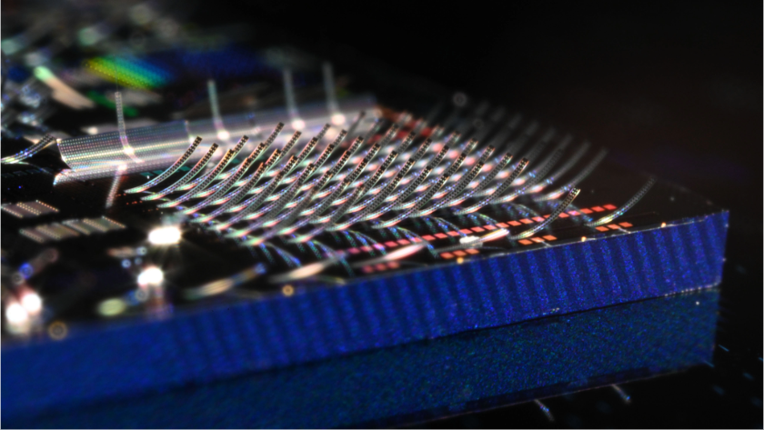
A new class of photonic chips uses “ski jump” structures to beam light into free space, enabling larger quantum computers and ultra-high-resolution displays.
Photonic chips are reshaping digital electronics by using light, rather than electricity alone, to process and move data.
Compared to their electronic counterparts, photonic chips deliver lightning-fast communication speed and greater bandwidth by relying on light. But because light travels through optical wires in most chip-scale systems, much of the light remains trapped inside the chip.
If that light could be efficiently transmitted off the chip and into the outside world, it could set the stage for dramatic advances in quantum computing, ultra high-resolution image displays, compact LiDAR (Light Detection and Ranging) systems, and faster, more powerful 3D printing.
A team of researchers has developed a new class of photonic chip that can beam light off the chip and into free space in a scalable way. This chip-to-world photonic interface could unlock opportunities for machine vision and intelligence across applications, including autonomous vehicles, robotics, augmented reality, biomedical imaging, and laser-based lithography.
The technology was developed through a collaborative research effort funded by the MITRE Quantum Moonshot program. The findings appear in the journal Nature, co-authored by researchers from The MITRE Corporation, the Massachusetts Institute of Technology (MIT), the University of Arizona, Sandia National Laboratories, and the University of Colorado Boulder.
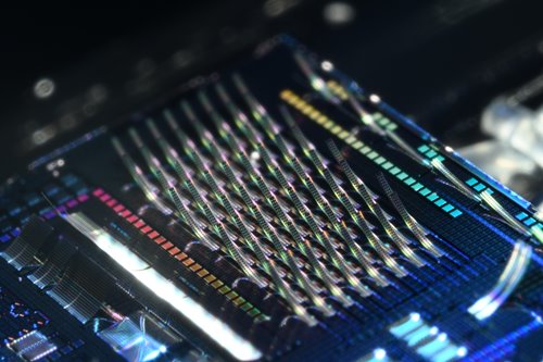 The research team was able to fabricate an array of microscopic structures that curl upward from the chip, resembling tiny, glowing “ski jumps.” Image: MIT
The research team was able to fabricate an array of microscopic structures that curl upward from the chip, resembling tiny, glowing “ski jumps.” These ski jumps direct light traveling through the chip into free space, allowing researchers to control emissions from thousands of structures simultaneously.
The research team was able to fabricate an array of microscopic structures that curl upward from the chip, resembling tiny, glowing “ski jumps.” Image: MIT
The research team was able to fabricate an array of microscopic structures that curl upward from the chip, resembling tiny, glowing “ski jumps.” These ski jumps direct light traveling through the chip into free space, allowing researchers to control emissions from thousands of structures simultaneously.
“Because we’re able to emit the light directly from the surface of the chip, we could think about completely fiberless chip-to-chip optics. We could now network directly from one chip to another chip in free space,” said Henry Wen, a visiting research scientist at MIT’s Research Laboratory of Electronics (RLE), a research scientist with MITRE, and co-lead author of the paper on the new platform.
Wen said this is the first platform that makes it possible to sculpt the three-dimensional structure of a device that can carry optical, electrical, and mechanical signals all at the same time on a chip.
“Any one of those would be interesting. But the three of those combined has the potential to be revolutionary,” he said.
Quantum computing is still experimental but presents the capability of solving highly complex problems—including calculations that would take traditional computers thousands of years to process—by leveraging the physics of quantum bits, or qubits. In this platform, those qubits are atom-sized defects in a diamond lattice.
Harnessing these microscopic qubits calls for the use of highly precise laser beams. But existing methods used to broadcast and steer light off a photonic chip typically allow for only a few beams at once.
Matthew Zimmerman, co-lead author of the article and principal hardware engineer for Quantum Moonshot, said the research team demonstrated that their chip can vastly scale up those methods by using the ski jumps to send multiple precision light pulses simultaneously to control the quantum states of large volumes of qubits.
“By tiling dozens or even hundreds of these devices on a single chip and integrating them with our existing on-chip photonic components, we could eventually control thousands or millions of qubits, which you need for a scalable quantum computer,” he said.
Squeezing the waveguides would allow the structures to bend and distort rather than stay flat, allowing the light to be manipulated, the researchers explored various methods of engineering that stress.
“This required us as a team to go back to Mechanics 101 and understand how all these different layers and materials, and how their stresses, stiffnesses and densities were all interplaying with each other,” Wen said.
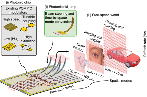 Piezoelectric photonic components process signals across time-bin modes, while “ski jump” emitters convert them into steerable free-space beams from the chip surface. Image: Nature
The team built the “ski jump” structures by layering two different materials that expand upon cooling. They added special patterns to each layer so the temperature change would cause the entire structure to curve upwards — an effect similar to the way thermostat coils curl and uncurl based on a room’s temperature to trigger the heating and cooling systems.
Piezoelectric photonic components process signals across time-bin modes, while “ski jump” emitters convert them into steerable free-space beams from the chip surface. Image: Nature
The team built the “ski jump” structures by layering two different materials that expand upon cooling. They added special patterns to each layer so the temperature change would cause the entire structure to curve upwards — an effect similar to the way thermostat coils curl and uncurl based on a room’s temperature to trigger the heating and cooling systems.
As waveguides on the chip direct light to the ski jump structures, the researchers then use a series of modulators to precisely control how the light is turned on and off — projecting light off the chip and into free space.
“You can project a full-scale image or video that in and of itself is about the size of a single pixel on an iPhone,” Greenspon said.
Worth noting, Zimmerman said, is that the device projecting those ultra-high-resolution images isn’t much larger. “It’s coming from a device that’s basically the width of a human hair and a millimeter long. So it’s a very small footprint,” he said.
The same capability could be used to improve 3D printing speed and quality. “Using arrays of these scanners it's possible to take something that would have required several hours down to less than a minute, or even shorter,” Wen said.
Now that the team has demonstrated the ability to consistently fabricate an array of ski jump structures on a chip, potential next steps include integrating and coordinating multiple ski-jumps in that array on a single photonic chip to do larger-scale image projection and qubit control, and potentially collaborating with other groups that are interested in a scalable platform, Greenspon said.
Wen said the team has been in conversations with potential investors but is also looking to connect with domain-area experts who have a use for large-scale laser beam control.
“If there are people who are equally passionate about this technology approach, we’re interested in hearing from you,” Wen said.
Autumn Giusti is an independent writer in New Orleans.
Compared to their electronic counterparts, photonic chips deliver lightning-fast communication speed and greater bandwidth by relying on light. But because light travels through optical wires in most chip-scale systems, much of the light remains trapped inside the chip.
If that light could be efficiently transmitted off the chip and into the outside world, it could set the stage for dramatic advances in quantum computing, ultra high-resolution image displays, compact LiDAR (Light Detection and Ranging) systems, and faster, more powerful 3D printing.
A team of researchers has developed a new class of photonic chip that can beam light off the chip and into free space in a scalable way. This chip-to-world photonic interface could unlock opportunities for machine vision and intelligence across applications, including autonomous vehicles, robotics, augmented reality, biomedical imaging, and laser-based lithography.
The technology was developed through a collaborative research effort funded by the MITRE Quantum Moonshot program. The findings appear in the journal Nature, co-authored by researchers from The MITRE Corporation, the Massachusetts Institute of Technology (MIT), the University of Arizona, Sandia National Laboratories, and the University of Colorado Boulder.
The research team was able to fabricate an array of microscopic structures that curl upward from the chip, resembling tiny, glowing “ski jumps.” Image: MIT
“Because we’re able to emit the light directly from the surface of the chip, we could think about completely fiberless chip-to-chip optics. We could now network directly from one chip to another chip in free space,” said Henry Wen, a visiting research scientist at MIT’s Research Laboratory of Electronics (RLE), a research scientist with MITRE, and co-lead author of the paper on the new platform.
Wen said this is the first platform that makes it possible to sculpt the three-dimensional structure of a device that can carry optical, electrical, and mechanical signals all at the same time on a chip.
“Any one of those would be interesting. But the three of those combined has the potential to be revolutionary,” he said.
Scaling up quantum computing
The Quantum Moonshot program is a collaborative effort including researchers from MITRE, MIT, Sandia and UC Boulder to develop the world’s first fully universal, scalable photonic quantum computer and integrated quantum network.Quantum computing is still experimental but presents the capability of solving highly complex problems—including calculations that would take traditional computers thousands of years to process—by leveraging the physics of quantum bits, or qubits. In this platform, those qubits are atom-sized defects in a diamond lattice.
Harnessing these microscopic qubits calls for the use of highly precise laser beams. But existing methods used to broadcast and steer light off a photonic chip typically allow for only a few beams at once.
Matthew Zimmerman, co-lead author of the article and principal hardware engineer for Quantum Moonshot, said the research team demonstrated that their chip can vastly scale up those methods by using the ski jumps to send multiple precision light pulses simultaneously to control the quantum states of large volumes of qubits.
“By tiling dozens or even hundreds of these devices on a single chip and integrating them with our existing on-chip photonic components, we could eventually control thousands or millions of qubits, which you need for a scalable quantum computer,” he said.
Mechanical problem-solving
Researchers needed a way to move light around in a manufacturable way from a chip. “We already knew our platform had this combination of waveguides. But prior to this, we were using them entirely in the plane of the chip,” Wen said.Squeezing the waveguides would allow the structures to bend and distort rather than stay flat, allowing the light to be manipulated, the researchers explored various methods of engineering that stress.
“This required us as a team to go back to Mechanics 101 and understand how all these different layers and materials, and how their stresses, stiffnesses and densities were all interplaying with each other,” Wen said.
Piezoelectric photonic components process signals across time-bin modes, while “ski jump” emitters convert them into steerable free-space beams from the chip surface. Image: Nature
As waveguides on the chip direct light to the ski jump structures, the researchers then use a series of modulators to precisely control how the light is turned on and off — projecting light off the chip and into free space.
Full images on a single pixel
Andy Greenspon, co-lead author of the paper and experimental quantum physicist at MITRE, said the pixel size for an array of ski jumps on a chip can shrink down to about 1 micron, which could enable lightweight, ultra-high-resolution augmented reality glasses or other imaging systems. A similar array could be used to shrink LiDAR systems, which are used in self-driving car technology.“You can project a full-scale image or video that in and of itself is about the size of a single pixel on an iPhone,” Greenspon said.
Worth noting, Zimmerman said, is that the device projecting those ultra-high-resolution images isn’t much larger. “It’s coming from a device that’s basically the width of a human hair and a millimeter long. So it’s a very small footprint,” he said.
The same capability could be used to improve 3D printing speed and quality. “Using arrays of these scanners it's possible to take something that would have required several hours down to less than a minute, or even shorter,” Wen said.
Now that the team has demonstrated the ability to consistently fabricate an array of ski jump structures on a chip, potential next steps include integrating and coordinating multiple ski-jumps in that array on a single photonic chip to do larger-scale image projection and qubit control, and potentially collaborating with other groups that are interested in a scalable platform, Greenspon said.
Wen said the team has been in conversations with potential investors but is also looking to connect with domain-area experts who have a use for large-scale laser beam control.
“If there are people who are equally passionate about this technology approach, we’re interested in hearing from you,” Wen said.
Autumn Giusti is an independent writer in New Orleans.
A new class of photonic chips uses “ski jump” structures to beam light into free space, enabling larger quantum computers and ultra-high-resolution displays.

Independent writer, editor, and content specialist.
Related Content


Aug 17, 2026
8 Strategies for Building a Smarter Career Path


Mechanical engineers can make smarter career pivots by planning ahead, building strong networks, and choosing opportunities that connect one move to the next.


Aug 14, 2026
Quiz: Behind the Shop Floor’s Machines

What do you know about the machines and processes that built modern manufacturing?


Aug 13, 2026
Podcast: Redefining Nuclear Power with Caroline DeWitte


Aug 12, 2026
Three Ventures from Africa and Three from the Americas Earn Places in Annual ASME ISHOW Cohort with Innovative Solutions to Address Energy, Food Storage, Healthcare, and Recycling Challenges